Mouse Mat : Semiconductor wafer, artwork F007 / 9912
![]()

Home Decor from Science Photo Library
Semiconductor wafer, artwork F007 / 9912
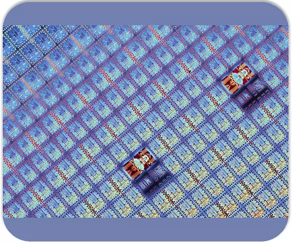
Computer enhanced image of a part of a semiconductor wafer. Wafers are divided up into blocks to make the integrated circuits ( chips ) used in electronic devices. Hundreds of thousands of transistors can be fitted on a single chip and connected by conducting pathways. The complex pattern of circuits that comprises each chip is built-up in a series of processes involving masks, deposition of insulators and etchings. Finished chips are eventually diced from the wafer prior to packaging
Science Photo Library features Science and Medical images including photos and illustrations
Media ID 9310949
© PASIEKA/SCIENCE PHOTO LIBRARY
Blue Chip Chips Circuits Component Conductor Data Electronic Electronics Futuristic Grid Integrated Circuit Microchip Part Semiconductor Silicon Silicon Wafer Transistor Wafer
Mouse Pad
Standard Size Mouse Pad 7.75" x 9..25". High density Neoprene w linen surface. Easy to clean, stain resistant finish. Rounded corners.
Archive quality photographic print in a durable wipe clean mouse mat with non slip backing. Works with all computer mice
Estimated Image Size (if not cropped) is 23.7cm x 16.5cm (9.3" x 6.5")
Estimated Product Size is 23.7cm x 20.2cm (9.3" x 8")
These are individually made so all sizes are approximate
Artwork printed orientated as per the preview above, with landscape (horizontal) orientation to match the source image.
EDITORS COMMENTS
This print showcases the intricate beauty of a semiconductor wafer, artwork F007 / 9912. Enhanced by computer technology, this close-up image reveals a part of the wafer used to create integrated circuits (chips) for electronic devices. The wafer is divided into blocks that house hundreds of thousands of transistors and are interconnected through conducting pathways. The complexity of each chip's circuitry is meticulously constructed through a series of processes involving masks, insulator deposition, and etchings. This delicate pattern forms the backbone of modern technology, enabling our electronic devices to function seamlessly. In this studio shot, the futuristic blue hue adds an element of sophistication and innovation to the composition. The grid-like arrangement highlights the precision required in manufacturing these chips while emphasizing their importance as data conductors. Silicon serves as the foundation for these components, allowing them to perform at optimal levels. As we explore this mesmerizing artwork further, we gain insight into how microchips are created - from their initial formation on silicon wafers to being diced before packaging. This photograph offers us a glimpse into the world behind our beloved electronics - reminding us that beneath their sleek exteriors lies an intricate network responsible for powering our digital lives.
MADE IN THE USA
Safe Shipping with 30 Day Money Back Guarantee
FREE PERSONALISATION*
We are proud to offer a range of customisation features including Personalised Captions, Color Filters and Picture Zoom Tools
SECURE PAYMENTS
We happily accept a wide range of payment options so you can pay for the things you need in the way that is most convenient for you
* Options may vary by product and licensing agreement. Zoomed Pictures can be adjusted in the Cart.


