Fraud Blocker Skip to main content

Silicon Collection (page 3)

Silicon, the versatile element that shapes our technological world

Background imageSilicon Collection: Citrine and amethyst

Citrine and amethyst are both varieties of quartz (silicon dioxide)

Background imageSilicon Collection: Agate

Agate
A cut and polished section of blue agate from Idar-Oberstein, Germany. Agate (silicon dioxide) is a cryptocrystalline quartz

Background imageSilicon Collection: Amethyst

Amethyst is the purple variety of quartz (silicon dioxide) and is a popular gemstone

Background imageSilicon Collection: Potentilla nivea L. snow cinquefoil

Potentilla nivea L. snow cinquefoil
Sketch 2, Newfoundland Volumes. From a collection of original drawings and sketches by Georg Dionysius Ehret (1708-1770). Held in the Botany Library at the Natural History Museum, London

Background imageSilicon Collection: Banded iron formation

Banded iron formation
3, 000 million year old specimen of banded iron-rich chert from the Murchison Goldfield, Western Australia. The banding derives from differing amounts and oxidation state of the iron composite

Background imageSilicon Collection: Quartz

Quartz
A quartz specimen (silicon dioxide) from San Juan del Rey, Minas Gerias, Brazil

Background imageSilicon Collection: A large cut citrine

A large cut citrine
Citrine is the yellow and orange variety of quartz (silicon dioxide). Specimen held at the Natural History Museum, London

Background imageSilicon Collection: Citrine and sapphire

Citrine and sapphire
Fine and poor examples of gem cutting and polishing. A superbly cut citrine (a yellow variety of quartz) and a poorly cut sapphire (blue), a variety of the mineral Corundum (aluminium oxide)

Background imageSilicon Collection: Quartz box and carved lizard

Quartz box and carved lizard
An ornamental box set with different quartz stones (silicon dioxide) including a large central citrine together with a carved lizard in cat s-eye quartz

Background imageSilicon Collection: Silicon Chip

Silicon Chip
An Integrated Circuit, (IC), more commonly known as a Silicon Chip, a vital component of all computers. Date: 1981

Background imageSilicon Collection: Silicon based life form, artwork

Silicon based life form, artwork
Silicon based life form. Artwork of an alien life form composed of silicon. Silicon is close to the element to carbon in the periodic table and has similar chemical properties

Background imageSilicon Collection: Silicon based life forms, artwork

Silicon based life forms, artwork
Silicon based life forms. Artwork of an alien landscape with life forms composed of silicon. Silicon is close to the element carbon in the periodic table

Background imageSilicon Collection: Analysing fuel oil for silicone traces

Analysing fuel oil for silicone traces
MODEL RELEASED. Analysing fuel oil for silicone traces, using an absorption spectroscope. Metal and silicone impurities in fuel oil can lead to problems such as inefficient combustion

Background imageSilicon Collection: Early Earth-like planet, artwork

Early Earth-like planet, artwork
Early Earth-like planet. Computer artwork of an alien (extrasolar planet), showing silicate crystals on its surface. As Earth-like planets cool

Background imageSilicon Collection: Artificial brains

Artificial brains. Conceptual computer artwork of brains being created from silicon circuits. This represents neuromorphic engineering

Background imageSilicon Collection: MEMS production, metal evaporation

MEMS production, metal evaporation
MEMS production. Inside of a metal evaporation machine that is being used to produce MEMS (microelectromechanical systems) devices

Background imageSilicon Collection: Photodiode

Photodiode. This is a type of diode that allows electric current to flow if the light levels are high enough. A diode is an electronic component that acts as a one-way valve for the flow of electric

Background imageSilicon Collection: MEMS production, chemical etching

MEMS production, chemical etching
MODEL RELEASED. MEMS production. Clean room technicians using chemical etching processes to produce MEMS (microelectromechanical systems) devices

Background imageSilicon Collection: MEMS production, furnace processing

MEMS production, furnace processing
MEMS production. Row of silicon wafers entering a furnace during the process of producing MEMS (microelectromechanical systems) devices

Background imageSilicon Collection: One of the Maluku islands in Indonesia

One of the Maluku islands in Indonesia
Semiconductor diode. Electronic component that acts as a one-way valve for the flow of electric current. Most diodes are semiconductor diodes

Background imageSilicon Collection: Compact flash memory card

Compact flash memory card. Flash memory is a form of non-volatile computer data storage. Flash memory cards may be used with digital cameras, handheld and mobile computers, telephones, music players

Background imageSilicon Collection: MEMS production, device sorting

MEMS production, device sorting
MODEL RELEASED. MEMS production. Tweezers being used by a clean room technician to sort MEMS (microelectromechanical systems) devices into waffle-box storage containers

Background imageSilicon Collection: MEMS production, support bonding

MEMS production, support bonding
MEMS production. Microscope apparatus being used to mount MEMS (microelectromechanical systems) devices onto support structures

Background imageSilicon Collection: Silicon nanowire device, held by tweezers

Silicon nanowire device, held by tweezers. This device is coated with billions of tiny nanowires, each measuring a few nanometres (billionths of a metre) in diameter

Background imageSilicon Collection: MEMS production, thin film deposition

MEMS production, thin film deposition
MODEL RELEASED. MEMS production. Clean room technician using a thin film deposition machine to produce MEMS (microelectromechanical systems) devices

Background imageSilicon Collection: MEMS production, plasma etching

MEMS production, plasma etching
MODEL RELEASED. MEMS production. Clean room technicians using plasma etching techniques to produce MEMS (microelectromechanical systems) devices

Background imageSilicon Collection: MEMS production, gold metal circuitry

MEMS production, gold metal circuitry
MEMS production. Wafer on which gold metal has been deposited to form electronic circuitry for MEMS (microelectromechanical systems) devices

Background imageSilicon Collection: Thermoelectric silicon nanowire, artwork

Thermoelectric silicon nanowire, artwork
Thermoelectric silicon nanowire. Computer artwork showing a silicon nanowire (centre) bridging two heating pads (top and bottom)

Background imageSilicon Collection: MEMS production, wafer cutting

MEMS production, wafer cutting
MEMS production. Machine being used to cut up a silicon wafer of MEMS (microelectromechanical systems) devices. The liquid provides lubrication during the cutting process

Background imageSilicon Collection: Semiconductor components

Semiconductor components
Semiconductors. Selection of various applications of semiconductors. Semiconductors are materials with properties between those of conductors and insulators

Background imageSilicon Collection: MEMS production, machined silicon wafer

MEMS production, machined silicon wafer
MODEL RELEASED. MEMS production. Machined silicon wafer being used for MEMS (microelectromechanical systems) devices, being held by a clean room technician

Background imageSilicon Collection: MEMS production, photolithography

MEMS production, photolithography
MODEL RELEASED. MEMS production. Clean room technicians using photolithography processes to produce MEMS (microelectromechanical systems) devices

Background imageSilicon Collection: MEMS production, hot embossing

MEMS production, hot embossing
MEMS production. Hot embossing machine being used to produce MEMS (microelectromechanical systems) devices. MEMS devices are constructed on a microscopic scale using technologies such as wet

Background imageSilicon Collection: MEMS production, quality control

MEMS production, quality control
MEMS production. Microscope being used to carry out quality control checks on a silicon wafer of MEMS (microelectromechanical systems) devices

Background imageSilicon Collection: MEMS production, flip chip bonding

MEMS production, flip chip bonding
MEMS production. Flip chip bonding apparatus (lower right) being used to mount MEMS (microelectromechanical systems) devices

Background imageSilicon Collection: MEMS production, external connections

MEMS production, external connections
MEMS production. Bonding machine and microscope being used to add the external connections to MEMS (microelectromechanical systems) devices

Background imageSilicon Collection: MEMS production

MEMS production
MODEL RELEASED. MEMS production. Clean room technician lifting a container of silicon wafers being used to produce MEMS (microelectromechanical systems) devices

Background imageSilicon Collection: Brain on a chip

Brain on a chip

Background imageSilicon Collection: Neural chip

Neural chip. Conceptual computer artwork of a neural network (centre) on a microchip. This could represent hardware which mimics such networks, or contains actual nerve cells

Background imageSilicon Collection: Macrophoto of silicon chips (linear motion effect)

Macrophoto of silicon chips (linear motion effect)
Integrated chips. Macrophotograph of high- performance microprocessor silicon chips, seen with a blurred " linear motion" effect

Background imageSilicon Collection: Coloured SEM of surface of an EPROM silicon chip

Coloured SEM of surface of an EPROM silicon chip
EPROM silicon chip. Coloured Scanning Electron Micrograph (SEM) of the etched surface of part of an EPROM silicon chip. Here

Background imageSilicon Collection: View of two silicon wafers with their chips

View of two silicon wafers with their chips

Background imageSilicon Collection: False-colour SEM connector wires on silic

False-colour SEM connector wires on silic
False-colour scanning electron micrograph of a TM 2716 integrated circuit, or silicon chip, show- ing 2 connecting wires bonded to terminal pads on the edge of the device

Background imageSilicon Collection: Silicon wafers

Silicon wafers and chips. View of two processed silicon wafers (upper right and lower left). The wafers contain dozens of identical microcircuits, which appear as squares

Background imageSilicon Collection: Coloured SEM of a single-electron transistor

Coloured SEM of a single-electron transistor
Single-electron transistor. Coloured scanning electron micrograph (SEM) of a single-electron transistor. Like the larger transistors it is designed to replace, it has three parts

Background imageSilicon Collection: Fabrication of integrated circuit wafers

Fabrication of integrated circuit wafers
Visual inspection of a photomask used in the fabrication of integrated circuit wafers at Seagate Microelectronics Ltd, Livingston, Scotland

Background imageSilicon Collection: Visual inspection of photomask

Visual inspection of photomask

Background imageSilicon Collection: Computer memory chip

Computer memory chip. This is a 144 pin SDRAM (synchronous dynamic random access memory) chip


All Professionally Made to Order for Quick Shipping

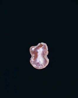
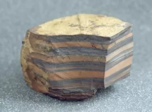
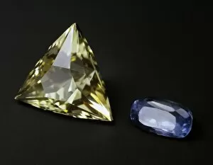
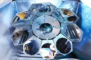
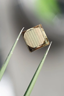
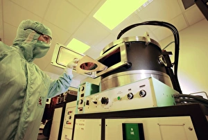
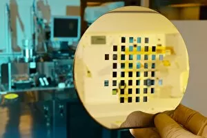
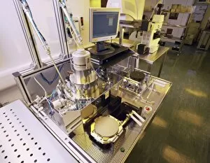
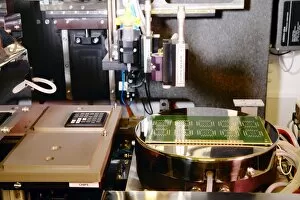
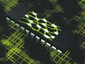
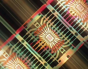
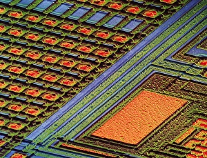
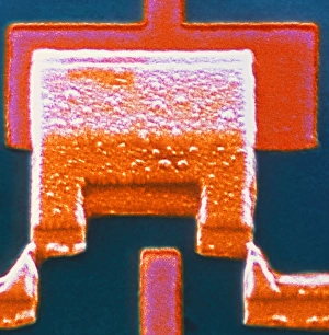
Silicon, the versatile element that shapes our technological world. From its mesmerizing crystal structure to its vital role in microchips and solar panels, silicon is truly a marvel of nature's ingenuity. In the depths of Earth's crust, silicon forms intricate crystals that captivate with their beauty. Under the lens of a light micrograph, these structures reveal themselves as delicate masterpieces, reminiscent of jasper or agate bowls adorned in shades of grey and white. But it is not just aesthetics that make silicon so remarkable. Its practical applications are boundless. In the realm of technology, we find silicon at the heart of every microchip connecting wire. Examined under an electron microscope (SEM), this tiny wire becomes a gateway to innovation and progress. Harnessing the power of sunlight, silicon finds another purpose in solar panels basking in the sun's rays. As photons strike its surface, electrons are set into motion, generating clean energy for our ever-growing needs. Even within teletext boards lies hidden artistry - an X-ray reveals a complex network etched onto a silicon chip. This intricate design represents countless lines of code and information flowing through circuits unseen by our naked eye. Venturing beyond technology, we discover stunning mineral formations where copper dances with quartz amidst Cornwall's rich landscapes. Cuprite with minor quartz from Gwennap showcases nature's ability to create harmonious compositions while chalcopyrite with quartz and minor sphalerite unites elements in perfect balance. The Cooks Kitchen Mine brings forth chalcocite alongside quartz – a testament to Mother Nature’s artistic prowess deep within England’s soil. Galena intertwined with quartz from Derbyshire adds an air of mystery as its exact origin remains uncertain. Lastly, copper embraces quartz at South Caradon Mine while chalcopyrite adorns dolcoath mine – both sites serving as reminders that beneath Earth’s surface lie treasures waiting to be discovered.